Test Wafer Center (TWC)
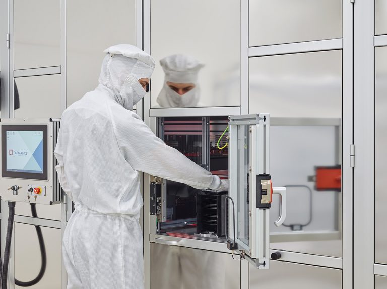
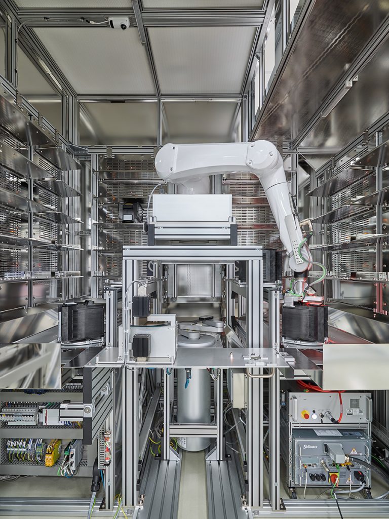
This all-in-one test wafer management solution is a key component of the intricate material logistics needed for preparation, qualification and reclaiming flows ensuring the quality of the fab’s output. It enables you to fully automate the kitting, storage, re-sorting, and de-kitting of test wafer lots.
Automated test wafer management in semiconductor production
Test wafers are indispensable for semiconductor manufacturing, crucial for equipment qualification and process monitoring. They constitute up to 50% of a fab’s wafer inventory. Managing test wafer lots manually is time-consuming and prone to errors.
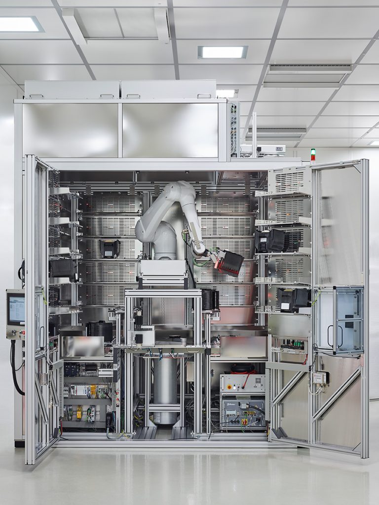
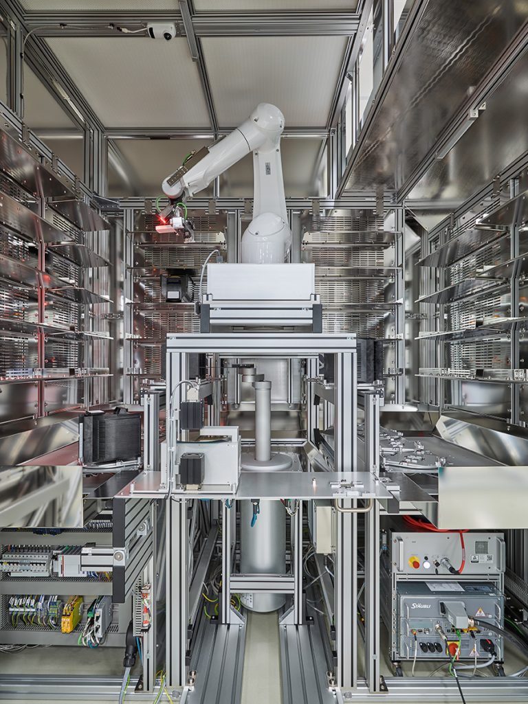
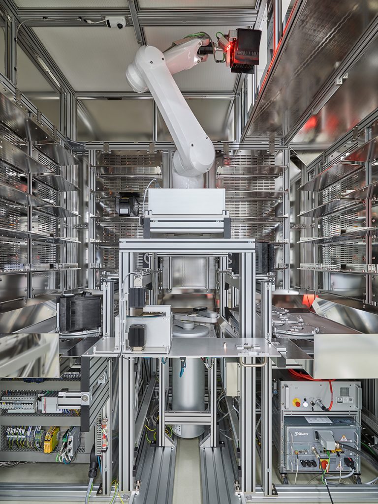
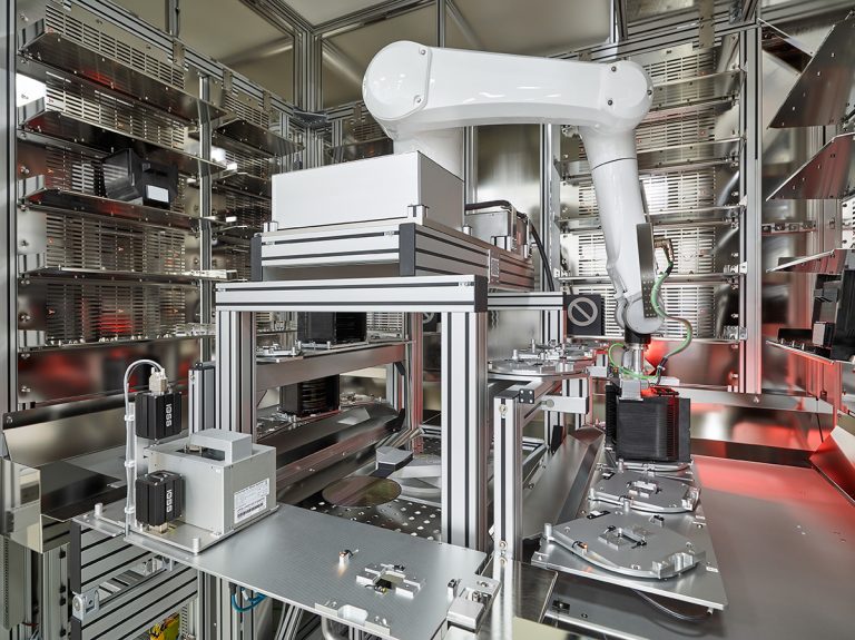
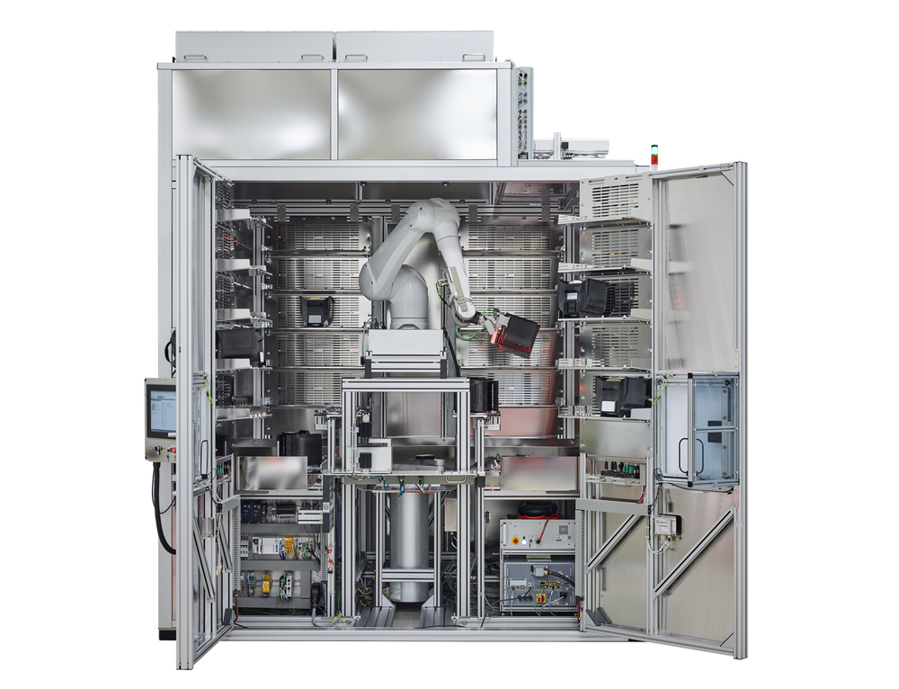
The Test Wafer Center (TWC) fully automates kitting and de-kitting of test wafer lots as well as their storage. Its compact and highly flexible layout allows up to 93 storage bins and up to 14 material handling locations making it the perfect solution for complex equipment qualifications scenarios. It gives you complete (remote) control for determining timing and content of each test wafer lot & enables just-in-time delivery to your process equipment.
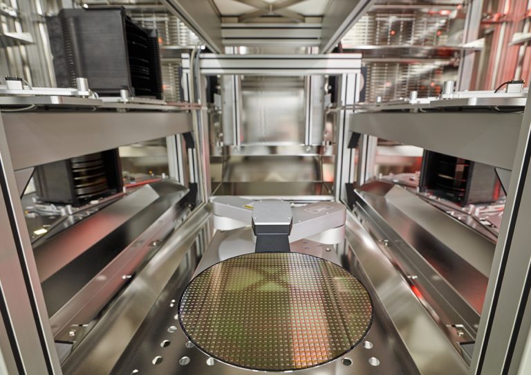
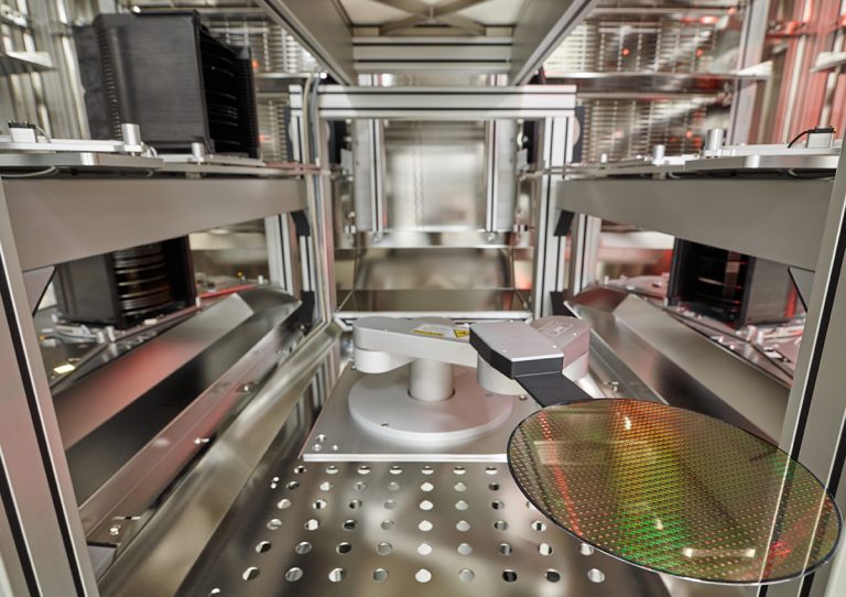
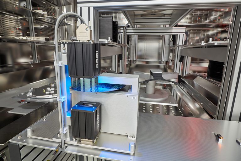
Featuring SECS host communication, camera-based robot routing, optional wafer alignment & identification, and various carrier identification options, the TWC ensures safe, accurate, & fully traceable material control.
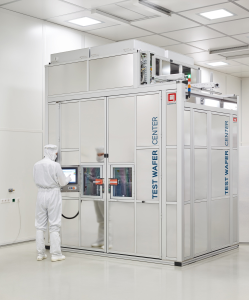
Connecting to any Automated Material Handling System (conveyor or vehicle based) as well as allowing manual carrier input or output, the integration with your fab is seamless & quick
Key features and benefits
Speed & Efficiency
- Commissions test & qualification lots fully automated, just-in-time and with complete traceability
- Reduces carrier transfers freeing up AMHS or manual transport capacity
Cleanliness & Material Protection
- Operates within its own ISO 3 mini environment, suitable for gray space installations & boasting a dedicated ultra-clean wafer handling area
- Detects handling errors (cross-slotting, double slotting etc.) & data inconsistencies (missing wafer, extra wafer, wrong wafer)
Space & Footprint
- Frees up expensive cleanroom space with a centralized test wafer management solution instead of numerous scattered handlings tools
- Allows layout optimization with an advanced design ideal for tight spaces, suitable even for a wall or corner installation
Resource Optimization
- Builds a complete wafer history with uninterrupted substrate tracking per SEMI E90
- Features automated error recovery & speeds up maintenance procedures providing best-in-class OEE via its auto-inventory function
External Content
Please accept "External Media" cookies to see the content.
I accept the display of external media and the transfer and processing of personal data according to the privacy policy.
Technical Data
| Dimensions (LxWxH) | 2,840 x 2,040 x 3,491 mm (112” x 80” x 137”) |
| Weight | 2,500 kg |
| Substrate type | 200 mm wafers / 8“ wafers |
| Carrier type/capacity | Up to 93 open cassettes (2,325 wafers) |
| Internal handling ports | Up to 14 |

